Simple Accumulator powered Phono Stage
The Concept
The phono stage is designed for MM and MC cartridges. JFETs, BJT transistors and op amps were chosen over
tubes because transistors are suitable devices to handle very small signals in my humble opinion. Furthermore
they allow a small enclosure that can be placed right next to the tonearm. Opamps improved dramatically
during the last years and the old paradigm of a fundamental superiority of tubes or discrete solid state
circuitry over opamps in phono stages has to questioned.
A balanced design was chosen for several reasons:
•
it provides common mode rejection and hence is much less sensitive for the picking up hum or RF,
•
the headroom for input and output levels is doubled,
•
DC drifts are cancelled out,
•
even harmonics are cancelled out,
•
the power supply load is kept constant relative to the music signal. The first stage's transistors as well as
the op amps run at the same currents, but inverse in polarity.
On the other hand balanced designs have a signal / noise ratio 3db worse compared to similar single-ended
design and the number of components is almost doubled. Furthermore balanced designs sometimes are
considered being less precise than good single-ended designs. This is true if the parameters of the inverting an
non-inverting stages are allowed to shift around are not forced to perfect symmetry. The circuitry of the phono
stage ensures perfect symmetry by a really stable current source in the input stage, a floating RIAA network
and precision op amps in the output stage.
Thinking about the basic circuit configuration I was in doubt whether to prefer active or passive RIAA
equalization. I reviewed a number of schematics, questioned experts and finally decided in favor of a passive
equalization. So the phono stage is simply built up by two linear, flat frequency response amplifying stages
with the passive RIAA network between them (see phono stage schematic).
Input Stage
The input stage is designed free from negative feedback (NFB). For real high resolution the input stage must be
able to handle very small signals around 10
-9
volts. With high amounts of NFB the input stage is confronted
with the even much smaller voltage differences between non-inverting and inverting inputs. Therefore I am
afraid to loose definition in a NFB loop within the input stage. On the other hand distortion is not a major
concern having very small signals.
The input resistor depends on the manufacturers recommendation. For any MM cartridge the input resistor
should be set to 47kOhm. For a Benz Micro MC Gold and a van den Hul Frog I set the input resistors to
510Ohm without any capacitances.
The first stage was set up originally as an all-jFET differential amplifier with two cascoded pairs of low noise
2SK369 jFETs (Fig.2a). The cascode configuration provides a large bandwidth. It eliminates the so called Miller
effect which is the capacitive feedback from drain to gate electrode of the jFET. This effect limits the upper
frequency in a common-source circuit. The 2SK369s were chosen because of their exceptional
transconductance of 40mA/V that was not matched by any other low noise jFET I could find browsing though
the data sheets. In general, the larger the transconductance figure for a device, the greater the gain it is
capable to deliver, when all other factors are held constant. The circuit provides enough slew rate and
headroom to handle the boosted high frequency signals without any risk of overdrive.
However, in listening tests we found that bipolar transistors such as the BC550C as upper cascode transistors
performed significantly better compared to jFETs (Fig.2b). In this circuit BJTs might be more ideal upper
cascode devices due to their lower effective impedance. The upper device in a cascode should ideally hold the
voltage across the device absolutely constant, regardless of current flow.
Independent from jFETs or BJTs as upper transistors, the gain is 100 (40db) at the differential output (between
a and b) and 50 from a or b to ground. This corresponds almost perfect to the theoretical gain according to the
following equation.
Gain = dI
D
/ dV
GS
x R
D
(EQ 1) *
dI
D
= drain current swing
dV
GS
= grain / gate voltage swing
(dI
D
/ dV
GS
) = transconductance = 40mA/V for the 2SK369
R
D
= drain resistor = 2.5kOhm
* EQ 1 is a simplified approximation and is valid only if the dynamic resistance of the cascode configuration is much larger than R
D
Bandwidth ranges from zero to 700kHz (-3db). The balanced design has the advantage of a doubled dynamic
range compared to a single ended design and allows more than 100mV
pp
input voltage without before
clipping. The schematic shows a non-balanced input variant of the circuitry. Real symmetry at the input can be
achieved easily by slight modifications at the input.
Signal symmetry of the input stage is ensured by a cascoded current source (CS) with a low noise RF bipolar
transistor BFR91and a 2SK369. The BFR91 can be considered a very high impedance source resistor of the jFET.
The differential resistance of a cascoded CS is several GigaOhm and hence substantially higher than that of a
normal jFET as a current source. The current source forces current swings of the two cascodes to perfect
mirror images. Hence the differential input stage cancels out even harmonic distortions. Second harmonics
are preferentially generated by FETs due to their square law responses. Another advantage of using a current
source is the absolutely constant load of the power supply.
RIAA Equalization
RIAA equalization is implemented by a floating low impedance network behind the differential input stage.
Virtually the frequency dependent components of the network are in parallel to the 2.5kOhm drain resistors
and form frequency dependent loads at the drains. Interestingly the network has not a single resistor in the
direct signal path.
The equalization tailors the frequency response to fit that of the RIAA curve by varying the drain load and
hence the amount of gain of the input stage according to the above equation EQ 1. Thus the RIAA network
controls the first stage gain, but without any component in the primary signal path. Furthermore the input
stage has less problems with slew rate limitations because the higher the frequency the lower the load and
hence the amplitude (fig. 3).
The passive equalization of an earlier MK I version of the phono stage looked quite similar but functioned entirely
different. The older version also had drain resistors of 2.5kOhm but a conventional voltage dividing network (fig. 4a,
4b).
After listening tests with the two different RIAA network designs we found the low impedance network (fig. 4b)
performed significantly better compared to a high impedance network although the RIAA responses measured
are almost identical (see RIAA plots).
The RIAA reproduction standard specifies three equalization time constants, 3180µs, 318µs and 75µs.
Theoretical RIAA response can be derived from the following equation:
db = 10log
10
(1+(1/4p
2
f
2
t
2
2
)) - 10log
10
(1+(1/4p
2
f
2
t
1
2
)) - 10log
10
(1+(4p
2
f
2
t
3
2
)) (EQ 2)
t1 = 3180µs time constant
t2 = 318µs time constant
t3 = 75µs time constant
Contrary to most commercial RIAA networks, a fourth time constant around 3.14µs was added to the network.
The Neumann cutting amp manual states a roll off at about 50kHz to stop the treble boost and Neumann
cutting lathes and amps are somehow Industry Standard. Therefore some authors claim that the commonly
documented RIAA curve is incorrect, because that roll off is neglected (see comments on fourth time constant).
In my RIAA I fitted an additional resistor in series with the small capacitor (time constant 75µs) to form a new
time constant around 3.14µs to compensate for the roll off at 50 kHz (Fig.3a and b). However, pros and cons of
that fourth time constant are discussed controversially For those who a fluent in German language there is an
interesting comment by Thomas Hartwig from THEL audio.
All RIAA capacitors are basically simple 10 % tolerance MKS types. I bought a bulk of thirty 100nF capacitors
(which was around 10 Euro) and took the time to hand-match the capacitors between the two channels to an
overall difference of less than 0.1 %. This is highly recommended, as stereo imaging relies on accurate channel
balance. Please note, that cheap digital meters may be quite inaccurate with regard to absolute values, but are
very useful to precisely match the relative values of capacitors.
The RIAA error remains within less than +/- 0.2db of the usual specification except around 20 kHz and above
due to the added fourth time constant. All grey colored resistors in the schematic, including the drain resistors
and the resistors at the non-invertig inputs of the op-amps are part of the RIAA network.
The 1µF coupling capacitors are Mundorf Mcap ZN caps. They also have to be matched carefully to achieve
equal impedances and symmetrical roll off at the low frequency end.
Output Stage
The second stage uses jFET-input precision op amps for further amplification of the signals tamed by the RIAA
network. High input impedances are necessary to avoid divergences from the RIAA. Minimum offset is
indispensable for (almost) DC-free primary windings of the LL 1570 XL line transformers. I chose OPA637 as a
good compromise of low noise, high input impedance, high speed and minimum offset. The gain is set to 30
(30db) for MM cartridges. For MC cartridges I recommend a gain around 300 (50db).
For MM applications you can either use OPA637 or OPA627. The latter one is much easier to get over here in
Germany. However, for MC applications you must use OPA637 because bandwidth of the OPA627 becomes
insufficient at high gains (see Tab.1) due to its internal unity gain stability compensation. Swapping between
OPA627 and OPA637 at a gain around 50db is clearly audible which emphasizes Allen Wright’s (see
www.vacuumstate.com) statement of a must of a minimum bandwidth at least one decade beyond the
accepted audio range for sufficient phase accuracy.
Listening Impressions
Comments and critics on audio circuits by the designer himself will always be subjectively and heavily biased.
However, from listening impressions the phono stage was considered being detailed, with good sound-staging,
good bass definition and especially a natural reproduction of human voices. It seriously can compete with
commercial products.
Back to Top of the Page
Back to main page
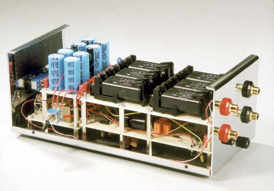
Fig. 1: Prototype of the phono stage. The switch at the side was added temporarily for listening tests
concerning a class A mode of the OP amps.
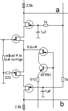
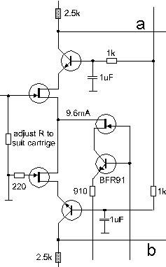
Fig.2a:
All FET input stage
Fig.2b:
FET / BJT input stage
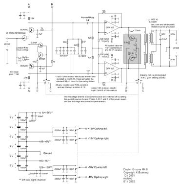
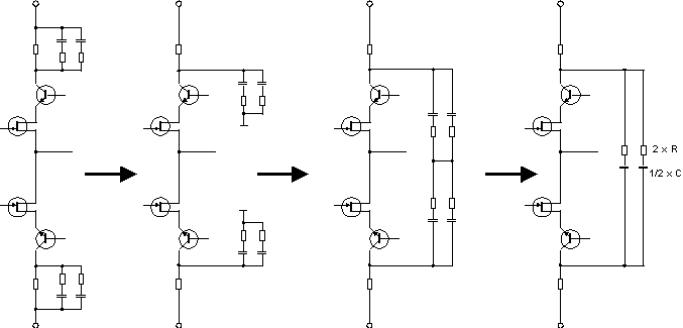
Fig. 3: The schematic
illustrates that the
resistors and capacitors
of the RIAA network are
virtually in parallel with
the drain resistors.
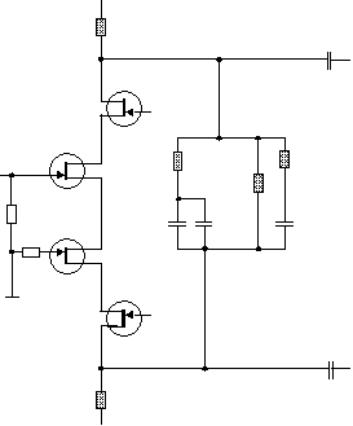
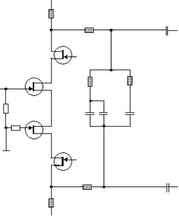
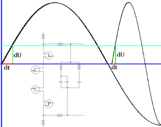
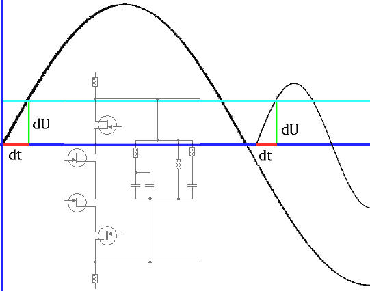
Fig.4a: „conventional“ RIAA network of old MK I phono stage. With a constant drain resistor and a voltage dividing
passive RIAA network following, the amplification of the input stage must be linear, i.e. independent from the
frequency. High frequencies plus high amplitudes (inverted RIAA on the LP !) given, the circuit has to be able to
perform high voltages changes dU (green) within a short time dt (red). Slew rate (dU/dt) limitations might degrade
the sonic performance at high frequencies.
Fig.4b: RIAA network of actual phono stage. With the RIAA network itself as a variable drain load, amplification
decreases with increasing frequency according to the RIAA curve. Hence less slew rate (dU/dt) is required for a full
performance of the circuit at high frequencies.
super triode, vinyl, audio, analog, single ended, SE, power amplifier, hybrid, tube, KT66, 6SN7, ECC88, Mosfet, Lundahl, MC phono stage, preamplifier, MM, MC, moving coil, moving magnet, LL1693, LL1667, LL9226, LL1933, RIAA, folded
cascode, 2CS5200, MAT12, 2N3810, LL1660S, IXFN32N120P, balancing amplifier